
STT-MRAM is a persistent memory solution that enables higher density with the ability to scale while consuming less power. With fast read/write speed similar to DRAM and the ability to handle memory workloads, STT-MRAM is considered the “leading contender for universal memory,” the “world's fastest write speed for embedded memory,” or as we like to say, “the industry’s most durable, highest performance persistent memory.” There’s no question STT-MRAM is highly regarded for its versatility, reliability, speed and endurance, especially for applications where data persistence is paramount, such as enterprise storage, industrial and transportation systems. For example, IBM has adopted Everspin STT-MRAM for use as a persistent write buffer in the flash modules used to build their All Flash Arrays (AFA).
Let’s peel back the covers to reveal the developments that allowed Everspin to achieve production status of a 1Gb persistent memory with a DDR4-like interface. In order to bring an innovative technology to a stage of consistent yield and high reliability, an in depth understanding of materials, process integration, and control of the variation of critical steps in the process is required. I’ll highlight a few of these here.
- Easy to integrate with standard complementary metal–oxide–semiconductors (CMOS), needing only 3 additional levels to construct the bit cell. For further chip density, the 1Gb cell is constructed with on-axis integration providing a vertical stack for array area efficiency.
- Materials are designed for reliable switching with narrow distributions as seen in the figure below:
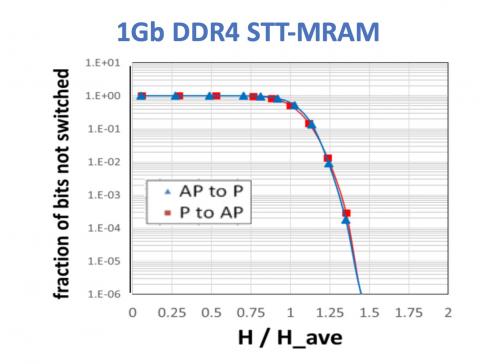
- The field switching distribution correlates to the resistance to thermal fluctuation
- The large separation from 0 field indicates essentially zero probability of spontaneous flips
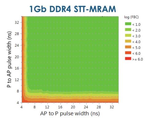
- Improved switching efficiency with zero fails over a range of pulse widths of ≥ 6-8 ns for 1Gb
- Endurance is better with longer pulses due to the lower required write bias
- Reduction in extrinsics for better BER at the end of the endurance life
- Full array cycling with stress to accelerate fails. Used bias and temperature acceleration to predict endurance at operating conditions. Product endurance >1e10 cycles to BER specification is demonstrated.
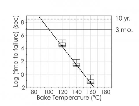
- Material composition and thickness optimized for data retention as measured by the energy barrier (Eb)
- Data retention bakes at 160°C were used to measure data retention flips with multiple bit sizes and fit to obtain Eb
- Baked parts at elevated temperature to accelerate fails. Free layers engineered to achieve desired data retention. 10yr @ 85C data retention has been achieved for 1Gb parts.
The STT-MRAM revolution has started with Everspin taking the lead. We have successfully transitioned STT-MRAM from R&D to volume manufacturing. There are now multiple ecosystem partners – Xilinx, Phison, Sage Electronics, Cadence Design – providing either FPGA, design IP or flash controller support for our breakthrough technology. Everspin has ushered in the era of Gigabit MRAM and we continue to lead in advanced development to realize the vision of universal memory.
Sanjeev Aggarwal, Vice President-Technology Research & Development at Everspin